Practice portal › Semiconductor Electronics › Digital Electronics and Logic Gates
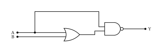
The truth table for the circuit given in the figure is [Figure: A and B feed an OR gate; the OR output and A feed a NAND gate giving Y. Options list Y for AB=00,01,10,11: (a) 1,0,0,0; (b) 0,0,1,1; (c) 1,1,0,0; (d) 1,1,1,1.]
Asked in JEE Main 12th April 1st Shift 2019 · Gate combinations and truth tables
- (1) 1,0,0,0
- (2) 0,0,1,1
- (3) 1,1,0,0
- (4) 1,1,1,1
Answer: (3) 1,1,0,0
Step-by-step solution
Y=A(A+B)=A (absorption)
00→1, 01→1, 10→0, 11→0.
Why the other options are wrong
- (1) This is NOR.
- (2) This is A; forgets the NAND bubble.
- (4) The output is 0 when A=1.
Reading this solution needs no sign-in. You only sign in to practise against the clock and keep your progress.
Practise this with a timer