Practice portal › Semiconductor Electronics › Zener Diode as a Voltage Regulator

Take the breakdown voltage of the zener diode used in the given circuit as 6 V. For the input voltage shown in figure here, the time variation of the output voltage is (graphs drawn are schematic and not to scale) [Figure: input is a sine wave of peak ±10 V. It is applied through a series resistor R₁ to two identical Zener diodes connected in series back to back across the output V₀. Options: (a) positive half clipped flat, negative half unclipped; (b) positive half unclipped, negative half clipped flat; (c) both halves clipped flat at the same level; (d) unclipped sine.]

Asked in JEE Main 4th Sept 1st Shift 2020 · Zener characteristics
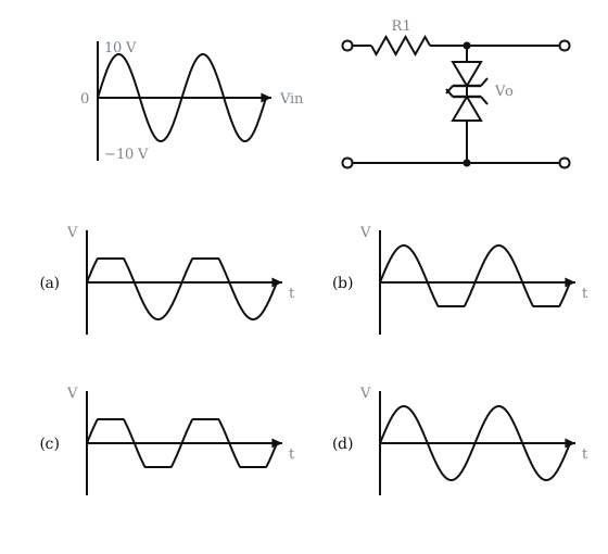
Figure: Zener characteristics
Answer: (3) Both halves clipped at the same level

Step-by-step solution

In each half-cycle one Zener is forward biased (about 0.7 V) and the other is in breakdown (6 V).

So the pair conducts once |Vᵢₙ| exceeds about 6.7 V, in either direction.

The output follows the input below that level and is clipped flat at about ±6.7 V: a symmetric clipped wave.

Why the other options are wrong

More Zener Diode as a Voltage Regulator questionsAll Zener Diode as a Voltage Regulator questions →

Reading this solution needs no sign-in. You only sign in to practise against the clock and keep your progress.

Practise this with a timer